What SiCarrier’s President Said at SEMICON China
Full transcript below. Find out more about who SiCarrier is
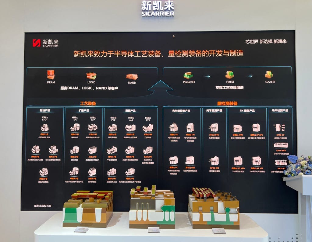
SiCarrier (新凯来), a rising semiconductor equipment company in China, made a high-profile debut at the 2025 SEMICON China exhibition. The introduction of a product portfolio featuring more than 30 semiconductor equipment products across six distinct categories caught many by surprise.
Background
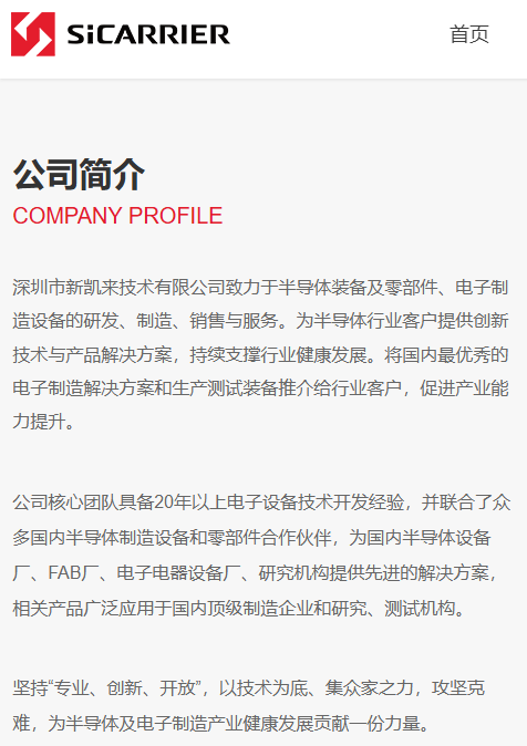
Founded in 2021, SiCarrier is wholly owned by Shenzhen Major Industry Investment Group, which is under the supervision of the Shenzhen State-owned Assets Supervision and Administration Commission (Shenzhen SASAC). Therefore, SiCarrier is a State-owned Enterprise (SOE) under the Shenzhen Government. Its core team includes veteran engineers with more than 20 years of experience from international giants such as ASML and Applied Materials.
Source: SiCarrier
There is market speculation that SiCarrier originated as a semiconductor equipment unit (2012 Starlight Engineering Lab) under Huawei, which was later spun off and acquired by Shenzhen SASAC. It has long been understood that Huawei’s investments in semiconductor equipment are primarily aimed at building a fully domestic, self-sufficient semiconductor equipment supply chain. A key indicator of SiCarrier’s rumored Huawei connection emerged when Li Zhoujian (郦舟剑), Head of Metrology at SiCarrier, appeared in a public interview. Notably, Li Zhoujian also serves as Vice President of Wireless R&D at Huawei and is 1 of 115 representatives for employee shareholders at Huawei. Under the Entity List by BIS, Huawei Starlight Engineering Department is listed as 1 of the aliases of SiCarrier although it is now wholly owned by Shenzhen Major Industry Investment Group.
Source: Huawei
Source: BIS
Core Products
SiCarrier’s debut “Famous Mountain Series” equipment covers the entire semiconductor manufacturing process, including:
Etching Equipment: The “Wuyi” Etch system supports advanced nodes below 7nm, using a proprietary electrostatic chuck design to significantly boost yield. It has capacitive couple plasma (CCP) system for dielectric etching and inductive couple plasma (ICP) for metal layer etching.
Diffusion Equipment:
“Emei” for Epitaxial
“Sanqing” for Rapid Thermal Processor / Annealing
Deposition Equipment:
“Putuo” PVD (benchmarked against AMAT’s Endura)
“Changbai” CVD (Chemical Vapor Deposition for 28nm to 5nm)
“Ali” ALD (for sub-5nm nodes)
Metrology & Inspection Equipment:
“Yuelu” BFI (Brightfield Patterned Wafer Defect Inspection)
“Danxia” DFI (Darkfield Patterned Wafer Defect Inspection)
“Penglai” PC (Unpatterned Wafer Surface Defect Inspection)
“Mogan” MBI (Mask Blank Defect Inspection)
“Tianmen” DBO and IBO (Overlay Measurement)
“Yimeng” AFM (Atomic Force Microscopy)
“Chibi” XPS (X-Ray Photoelectron Spectroscopy)
Tester Equipment
Chip Probing, Known Good Die and Final Testing
Photolithography: 28nm immersion lithography system (not directly showcased), with light source wavelength and overlay precision rumored to reach international standards
Source: SCMP
In my view, the more surprising development wasn’t the DUV immersion tool, but rather the progress in ALD, metrology, and inspection equipment. The emphasis on ALD suggests confidence in achieving a sub-5nm breakthrough. ALD plays a critical role in the transition to Gate-All-Around (GAA) architecture and eventually to CFET.
TSMC’s N2 node is reliant on the Gate-All-Around (GAA) architecture which will favor Atomic Layer Deposition (ALD) equipment and etching tool. ASMI is the biggest beneficiary of single-wafer ALD which will continue to grow in importance into CFET and 3D DRAM.
Metrology and inspection equipment has long been a key source of weakness in China’s domestic substitution efforts. These areas encompass a wide range of specialized equipment categories, making SiCarrier’s broad portfolio in this segment particularly noteworthy. Brightfield inspection is more complex than darkfield inspection and commands a significantly higher ASP for KLA. AFM is a niche metrology tool that will increasingly be adopted in the future. The main competition in this area in China is Skyverse which can cover Unpatterned Wafer Defect Inspection, Patterned Wafer Defect Inspection, 3D Surface Profiling Metrology, Film Metrology and Overlay Metrology.
Of course, the actual yield rates and readiness for mass production remain unclear. Another challenge for SiCarrier is the potential concern among Chinese customers about its rumored Huawei background. Huawei has a well-known history of vertical integration and a tendency to compete with its own suppliers and customers. The company is involved with a couple of fabs such as Fujian Jinhua (DRAM), Swaysure (DRAM), Qingdao Si'En (MCU, PMIC) and Shenzhen Pensun (28nm, 40nm foundry).
For Western WFE manufacturers like Applied Materials, Tokyo Electron, Lam Research, and KLA, progress in China’s domestic substitution efforts is inevitable. On the flip side, this shift may actually bring some reassurance to investors, as it reduces dependence on revenue from Chinese customers. SiCarrier will never be a threat to their global business as it is in the Entity List.
Another angle that investors often miss is how fast the China WFE manufacturers are ramping up in capabilities. Because of export control, YMTC has to rely on local manufacturer such as AMEC for etching tool. The top 3 WFE manufacturers in China (Naura, AMEC and ACM Research) have grown their revenue by more than 30% to USD 6 billion. Naura expects local WFE companies to grow their revenue from USD 8.2 billion in 2024 to USD 11 billion in 2025 (11% global market share). The 33% growth is very impressive, considering China WFE will be down 15-20% in 2025. Domestic import substitution rate for WFE will be 35% in 2025.
SiCarrier’s President Speech
SiCarrier’s President Du Liqun made a speech called Challenges and Opportunities in Semiconductor Process Equipment. Surprisingly, the direction that SiCarrier is pursuing is quite similar to what we have seen globally. PPAC remains the key focus of scaling, while 3D scaling is increasingly becoming more important than 2D scaling (Lithography).
PPAC and shift to 3D architecture:
Advancements in semiconductors consistently revolve around improving Power, Performance, Area, and Cost (PPAC). Innovations that reduce RC delays and further miniaturize transistors are crucial, with emerging technologies such as advanced lithography, selective deposition, and 3D architectures (like Gate-All-Around, GAA) being key pathways.Shift to Atomic-Level Precision:
With technology nodes progressing from 7nm toward 3nm, equipment precision, particularly in plasma and RF energy control, must improve dramatically by roughly tenfold. Atomic Layer Deposition (ALD) and Atomic Layer Etch (ALE) will increasingly be more important in the future.Integration of AI and Simulation Technologies:
AI and big data present substantial opportunities for optimizing semiconductor equipment operation, predictive maintenance, and process efficiency. SiCarrier emphasizes developing proprietary simulation software and control systems to exploit AI-driven insights fully, thus enhancing equipment performance and reliability.
Full Translated Speech
Source: 芯视点
Ladies and Gentlemen, good morning. First of all, I'd like to express my sincere gratitude to the organizers for providing this wonderful opportunity for us to gather in Shanghai during this vibrant spring season.
Today, it’s raining softly outside. As the proverb goes, "Good rain knows its season, arriving precisely in spring," and similarly, SiCarrier has emerged timely. At SiCarrier Industrial Machinery, our primary business focuses on process equipment and measurement instruments. Over the past few years, we have dedicated ourselves to technical preparations and product development. Today, I am delighted to represent SiCarrier and share some humble insights we've gained through these recent years.
The Fourth Industrial Revolution is approaching, with the AI industry creating significant opportunities for the semiconductor sector. In this context, the critical question is—how much can China's domestic semiconductor equipment industry contribute to the development of our semiconductor sector? What technical strengths can we contribute to promote collective industry progress?
Whether considering memory or logic advancements, PPAC (Power, Performance, Area, and Cost) remains an eternal pursuit we must continually address. Across Logic, DRAM, or NAND, each generation of semiconductor devices consistently improves PPAC performance by 10% to 50%.
Improvements in PPAC illustrate that semiconductor equipment and devices primarily tackle two major issues: First, reducing RC Delay by all possible means; second, further miniaturizing transistor sizes to fit more transistors within a given area. Accordingly, solutions primarily fall into three categories:
Firstly, developing new materials to enhance overall performance. From a dimensional shrinkage perspective, two primary technologies are relevant: advanced lithography techniques for further CD reduction and exploring non-optical technologies due to existing lithography limitations. Technique like SAQP (Self-Aligned Quadruple Patterning) is one such solution recognized across industry.
The industry is also addressing lithography overlay challenges by exploring selective deposition and other techniques. A potential route involves leveraging non-optical techniques, employing our process equipment to partially solve lithographic issues.
Thirdly, there's industry consensus that current 2D architectures no longer suffice, prompting exploration into 3D structures such as Gate-All-Around (GAA) technology for logic and NAND applications.
These pathways—from material innovation to practical engineering application—require joint industry efforts.
Due to CD shrinkage and multiple exposure processes, Atomic Layer Etching (ALE) and Atomic Layer Deposition (ALD) applications will increase significantly. However, using SAQP or similar techniques could increase the total number of process steps by approximately 20%, demanding parallel improvements in yield and process windows for equipment. Expanding these process windows would significantly enhance overall yield.
Moreover, the adoption of 3D structures introduces more complexity, combining selective processes like ALE and ALD, further challenging equipment capabilities.
In terms of new equipment technology, managing three types of energy requires significant enhancements across three dimensions:
First, we require greater precision in energy control, including plasma and thermal energy management.
Second, extensive ALD and ALE usage demands the productivity of equipment to increase exponentially.
Third, expanding the process window remains a perennial goal.
Taking plasma and RF energy management as examples, evolving from 7nm to 3nm technology necessitates a tenfold improvement in energy precision. Hardware circuits' delay synchronization and response speeds similarly must improve tenfold. For instance, we can seek to reduce the response times from 10 milliseconds to 1 millisecond.
Optimizing the process window involves structural adjustments alongside enhanced auxiliary analysis methods. Artificial intelligence driven tuning, big data analytics, and robust computational hardware raise new challenges for hardware and algorithms.
Plasma energy accounts for roughly half of our process equipment. Industry viewpoints typically split between simulation and experimental approaches, which have coexisted competitively for many years.
In the recent 2 years, leading firms have been acquired by major international and domestic corporations. This phenomenon underscores that plasma management inherently integrates forward design, simulation, and diagnostics. Profoundly understanding the first principles of chamber operations is essential for guiding precise future designs, motivating SiCarrier to develop plasma simulation software several years ago.
Our simulation capability spans from atomic physical models and chamber chemistry to reaction models and diagnostics. Our simulation software, "Wen Yuan," benchmarks against the industry’s highest accuracy standards. "Wen Yuan" is inspired by the poetry line, "Ask the stream why it's so clear, for it is fed by flowing waters."
While we've completed our simulation strategy, converting designs into reality remains challenging. Synchronizing RF sources, matchers, chucks, coil magnetrons, gas valves, and detectors with our equipment necessitates comprehensive integration, a path SiCarrier has thoroughly addressed from system design to hardware, components, and algorithms.
Regarding hardware responsiveness, shifting from traditional CVD/ETCH to ALD/ALE significantly raises demands on transient response and stabilization times.
How can equipment consistently deliver excellent ALD characteristics? Equipment control systems play a critical role. While PLC systems dominated previously, we increasingly see advanced processors and logical systems adoption. Achieving fast, accurate, and stable hardware performance remains a future imperative.
Recognizing this, SiCarrier has developed an entirely self-designed control system, substantially improving control capabilities compared to traditional PLC systems.
Looking ahead, expanding process windows remains challenging. Leveraging AI, from semiconductor equipment physics and design data to fab-wide operational and power consumption data, presents vast opportunities. Despite myriad parameters and process variables, full utilization remains untapped. Integrating big data with physical simulation models could drive intelligent optimization and predictive maintenance.
SiCarrier has strategically positioned itself for future AI-driven optimization and smart maintenance. We've achieved promising accuracy in lifecycle prediction for specific components—within ten days—based on their physical characteristics and process impacts, aiming for larger-scale models providing optimal client solutions.
Our overall design philosophy emphasizes synchronized advancement across processes, materials, and equipment. Through precision energy control, intelligent process window tuning, and rapid, stable, and precise control systems, we aim to accelerate technological and material evolution, facilitating finer process management.
Guided by this vision, SiCarrier has developed six categories of processing and inspection equipment, addressing diverse logic and memory scenarios while supporting future advancements.
Exploring semiconductor physics boundaries remains our relentless pursuit, representing an infinite horizon as semiconductor people. SiCarrier remains committed to our technological roots, hoping to collaborate innovatively with partners for mutual success, providing customers with novel choices.
Semiconductor world, new choices, SiCarrier. Thank you.

