This is Part 2 of our deep dive on Tokyo Electron. If you missed the Part 1, you can check it out here.
Deposition - Stable share in a growing market
Deposition equipment involves tool that deposits thin films on the wafer – including thermal oxidation furnaces, Chemical Vapor Deposition (CVD) reactors, Physical Vapor Deposition (PVD) sputtering tools, and Atomic Layer Deposition (ALD) systems.
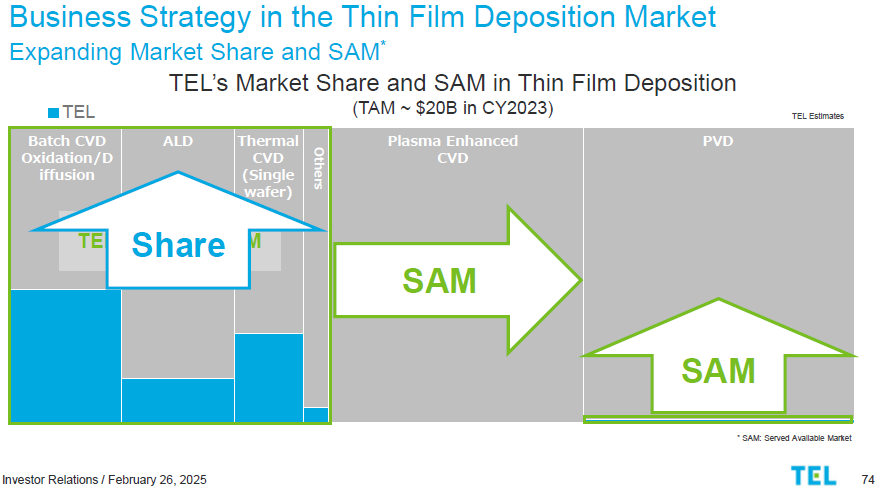
TEL has a comprehensive offering in deposition, historically rooted in batch oxidation / diffusion furnaces and CVD. According to TEL, its global market share in 2023 for overall deposition systems was 31% with major competitors including Applied Material, Kokusai and ASM International. TEL classifies its deposition into three types: Oxidation / Diffusion, CVD, and ALD. TEL held ~40% global share in oxidation / diffusion equipment, 40% in CVD, and 16% in ALD. For clarity, ALD refers to semi-batch or single wafer ALD, while oxidation / diffusion furnace is batch ALD.
Source: Tokyo Electron
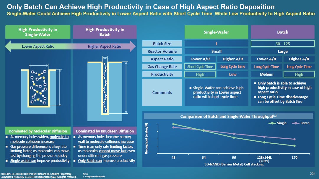
Starting with oxidation / diffusion furnaces, TEL’s main competitor is Kokusai in Japan. Kokusai has a dominant position in batch ALD for 3D NAND. As aspect ratio goes up with the layer race in NAND, there will be higher demand for batch ALD due to its higher productivity. As NAND producers work towards 300-400 layers, higher deposition will drive TAM growth which will benefit TEL’s revenue growth in deposition.
Source: Kokusai
Similarly in single-wafer ALD, Tokyo Electron faced a strong competitor in ASM International. ASM International is the dominant single-wafer ALD provider for advanced logic application with TSMC. With the adoption of Gate-All-Around (GAA) by TSMC at N2, ASM International will be a key beneficiary. TEL semi-batch ALD tool will find it tough to gain share in this space. TEL faced very strong competition from Kokusai and ASM International who are very focused on their core business of ALD.
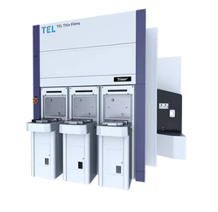
Triase is the key CVD product within Tokyo Electron’s deposition portfolio that has a high market share of 40%. The single-wafer CVD core focus lies in metal film deposition, particularly for Titanium Nitride (TiN) in DRAM electrode formation. Its Advanced Sequential Flow Deposition (ASFD) technology can deliver highly conformal, precisely controlled thin films through the use of sequential gas pulses with faster deposition rates than ALD. Operating at lower temperatures, it is also more suitable well-suited for temperature sensitive processes.
Triase, Source: Tokyo Electron
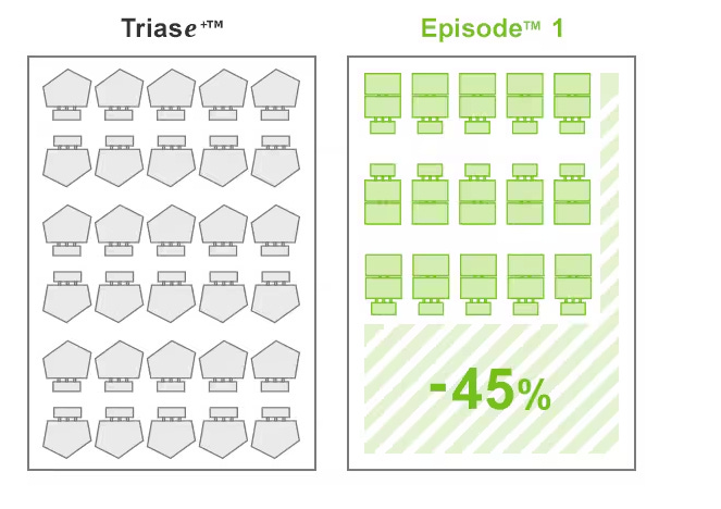
Tokyo Electron has introduced a new Episode 1 CVD equipment which has 45% smaller footprint than Triase. In addition, this new platform is able to integrate 8 process modules, which is twice that of Triase.
Source: Tokyo Electron
Etching - Gaining share in NAND conductor etching
Etching is a process that selectively removes material from a wafer's surface to create structures and patterns. Tokyo Electron is strong in dielectric etch with more than 50% share, whereas Lam Research leads in conductive etch (metals, polysilicon).
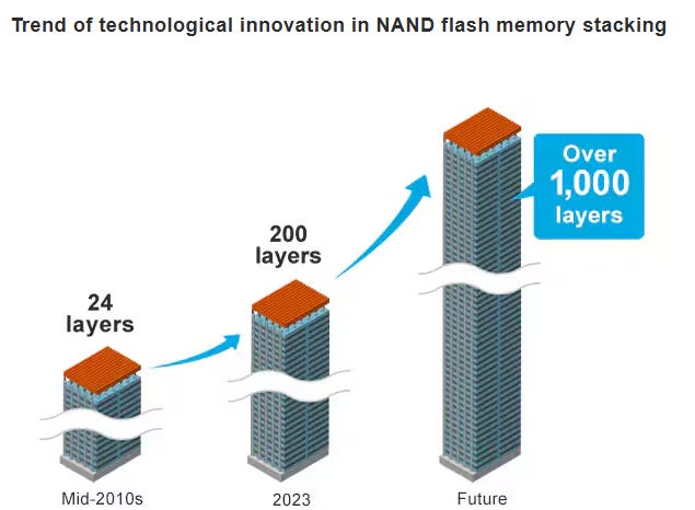
Etching is a particularly important process in 3D NAND as producers seek to increase the layer count. Scaling is done vertically by stacking memory cells vertically in a 3D architecture instead of shrinking transistor area through lithography. The challenge lies in the high aspect ratio (HAR) etching as the layer count increases at the trendline of 30% every 1.5 years. Aspect ratio is the height to width ratio when etching deep and narrow channel holes. Aspect ratio as high as 100:1 can lead to difficulties in achieving uniform etching. Tool productivity can also be another problem as doubling the layer count leads to doubling of the time taken for etching.
Source: Tokyo Electron
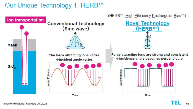
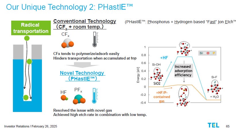
Recognizing the challenges posed by increasing HAR, TEL embarked on developing a novel etching technology in 2014. In 2023, TEL announced the new TELAVES cryogenic etcher. Notably, it achieves etch depths greater than 10 µm at rates 2.5 times faster than previous methods, while also reducing power consumption by over 40%. This is through the combination of High-Efficiency Rectangular Bias (HER) and Phosphorus + Hydrogen based Fast Ion Etch (PHastIE) technology.
Tokyo Electron's HER technology utilizes rectangular radio frequency (RF) wave to maintain a vertical ion incidence angle during the etching processes. Ion incident angle is varied in the conventional sine wave technology which results in bowing problem.
Source: Tokyo Electron
The PHastIE process leverages innovative chemistry and cryogenic temperatures to enhance high-aspect-ratio etching performance. By employing a novel process gas Hydrogen Fluoride (HF), deposition at feature openings is minimized, while the cryogenic environment effectively protects sidewalls during etching. This approach reduces bowing and increases etch rates.
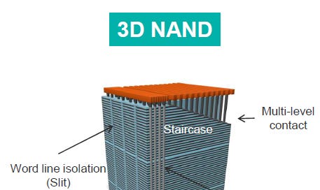
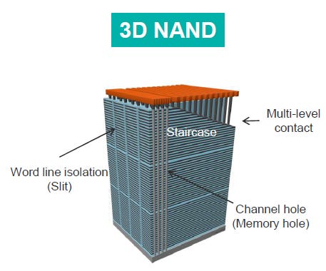
There are 4 key etching processes for 3D NAND
Channel Hole: Deep holes etched to form the transistors
Slis: Etched regions that isolate word lines, ensuring proper electrical functionality.
Multi-level Contact: Holes etched to establish connections between different metallic wiring layers.
Staircase: Connection for access to wordline in each layer
Today, TEL has high share in multi-level contact and word line isolation. Lam has almost 100% share for the extremely high aspect ratio channel hole etch in 3D NAND. TEL’s new cryogenic etcher breaks that monopoly, offering better throughput for 3D NAND of more than 400 layers. Samsung Electronics will be TEL 1st NAND customer using their cryogenic etcher for 400L 3D NAND. SK Hynix is also currently testing TEL’s cryogenic etcher.
For perspective, TEL projects that the conductor etch market for NAND is worth $2 billion in 2027. Assuming a 50% market share, this is an $1 billion incremental revenue for TEL. Lam Research is not sitting still as it has launched Cryo 3.0 in response. However, Lam Research is late to the cryogenic etcher game by 1.5 years and customers are incentivized to introduce a 2nd supplier to break the virtual monopoly. Kioxia is expected to be Lam Research’s Cryo 3.0 customer.
Bonder / Debonder - Exciting new opportunity
Wafer bonding equipment is used to fuse two wafers together – either permanently (for 3D stacking) or temporarily (for handling thinned wafers). Debonders remove temporary bonding materials so the wafer can be processed and later separated. This is a small but rapidly growing segment parked under the Prober segment for revenue.
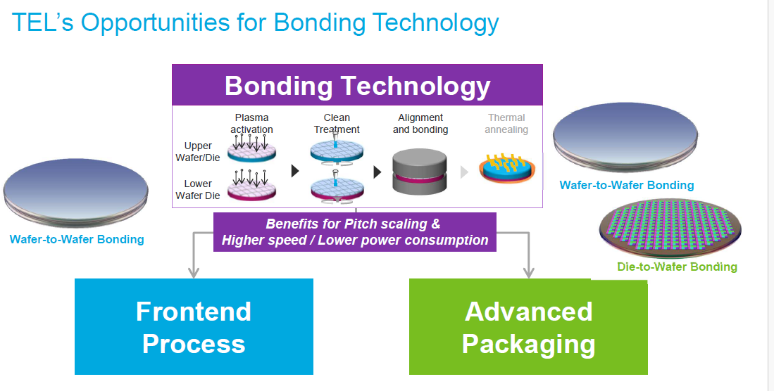
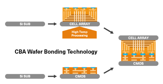
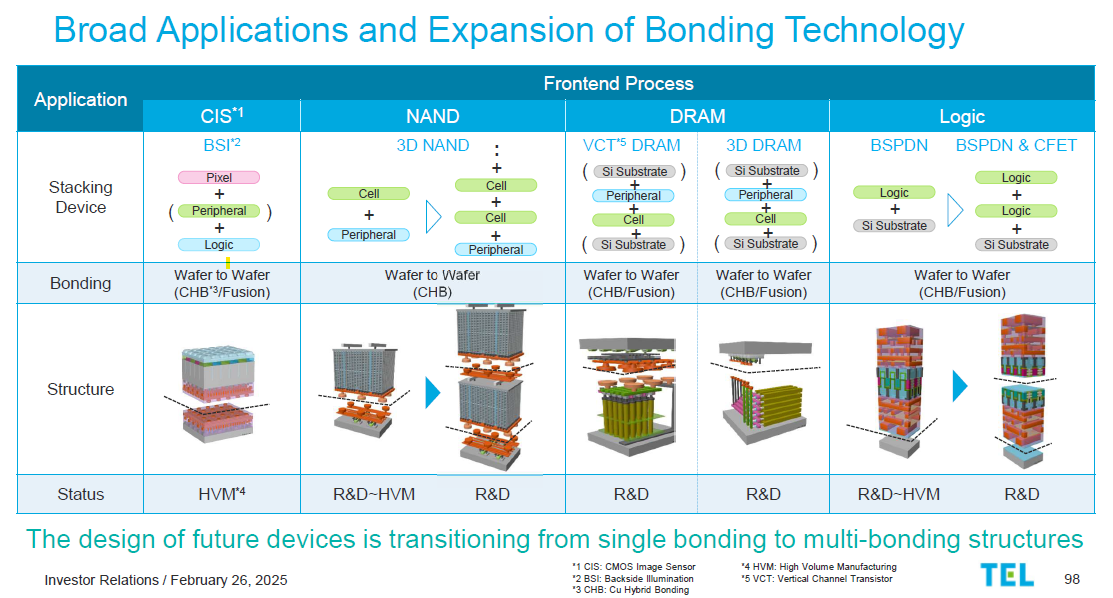
Lets start with permanent wafer bonding equipment which is also known as wafer-to-wafer (W2W) hybrid bonder. In W2W hybrid bonding, two fully processed wafers are precisely aligned and bonded together, establishing direct connections between their corresponding interconnects. This is currently in use for the production of CMOS image sensor. This is different from chip-to-wafer (C2W) hybrid bonding where individual dies are connected onto a target wafer without the use of traditional solder-based interconnects. Currently, BESI is the market leader for C2W hybrid bonder while EV Group is the market leader for W2W hybrid bonder.
Source: Tokyo Electron
W2W hybrid bonder is expected to experience strong growth this decade due to innovation happening in logic and NAND roadmap. Backside Power Delivery (BPD) will be adopted by Intel in 2025 and by TSMC for A16 in 2026. Traditional power delivery networks route power and signals through the front side of the wafer, leading to congestion and increased resistance as device scaling continues. BPD addresses this by relocating the power distribution network to the wafer's backside, thereby decoupling power and signal interconnects. W2W hybrid bonding is used to bond the front side of the 1st wafer to the carrier wafer for further processing.
Source: Applied Materials Masterclass on BPD
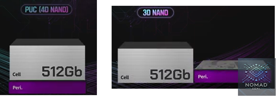
W2W hybrid bonding also enables the direct bonding of 2 wafers, placing the peripheral circuit under the memory cells for 3D NAND. This is similar to the innovative Xtacking technology adopted by YMTC that allows them to catch up to the competition. Through this peri under cell (PUC) technique, the chip size is reduced and the number of stacked layers can go up. Kioxia has adopted PUC in its Gen 8 BiCS technology and SK Hynix has sampled at 321L NAND.
Source: SK Hynix
Source: Kioxia
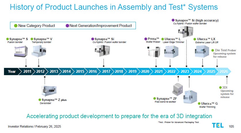
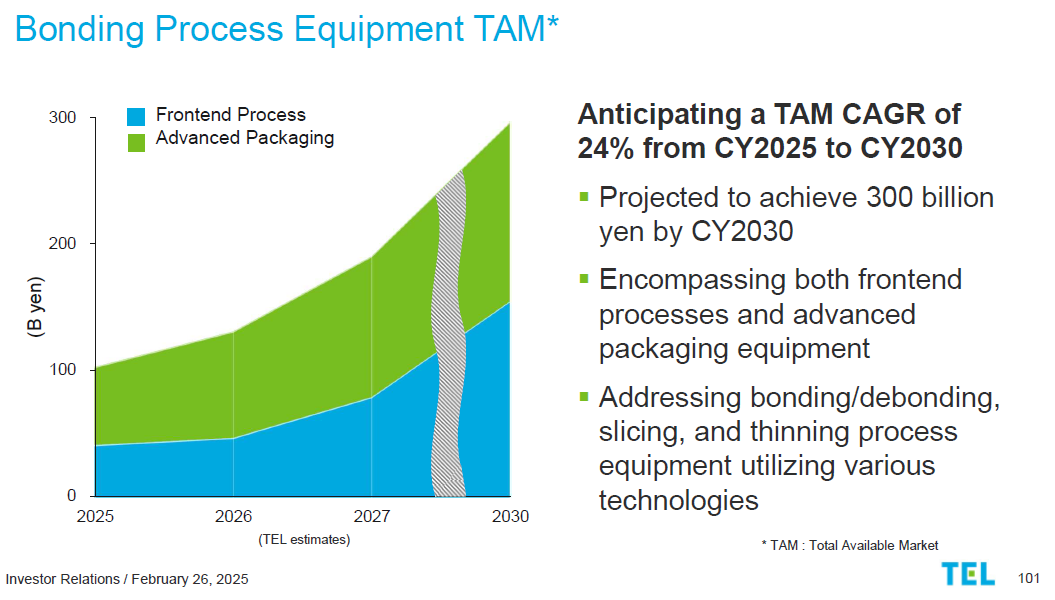
Beyond CIS, BPD and PUC, W2W hybrid bonding will be adopted for 3D DRAM in memory and CFET in logic. Tokyo Electron expects the market TAM for bonder to increase from JPY 100bn in 2025 to JPY 300 billion (USD 2 billion) in 2030. Currently, TEL has a 20% market share for W2W bonder with its Synapse Si bonder. If they can secure a market share of 20-40% in the bonder market, the revenue potential will be USD 400-800mn in 2030.
Source: Tokyo Electron
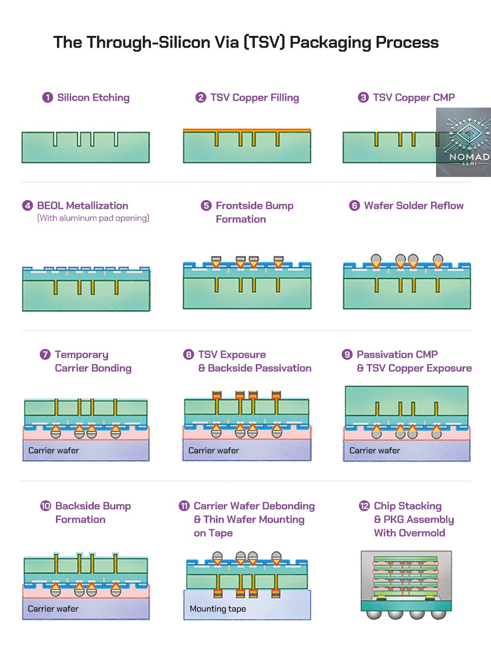
For the backend equipment, Tokyo Electron is the market leader for temporary bonder debonder. The biggest usage of temporary bonder debonder is currently for the HBM market. In order to stack multiple dies while maintaining the aspect ratio of through silicon vias (TSV), wafer thinning has to be carried out. The memory wafer has to be temporarily bonded onto a carrier wafer before it is thinned. To meet the 775um requirement for the HBM3e 12-Hi used in GB300, each individual chip has to be as thin as 32 um. After thinning is done, the wafer is then debonded and diced into individual dies. Tokyo Electron is the main supplier of temporary bonder debonder for SK Hynix, while German competitor SUSS Microtec supplies Micron and Samsung.
Source: SK Hynix
Cleaning - Relatively stagnant
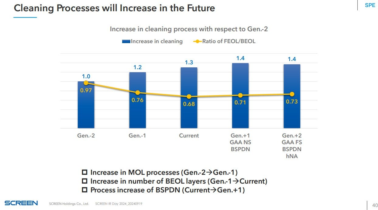
This is not an exciting segment given limited content growth and market share gain opportunity. As seen from the chart from Screen, the market leader in cleaning, there is a limited increase in number of cleaning step for N2 (GAA + BPD). While TEL may gain some market share from Screen, it is at risk of losing low to mid end market share to Chinese competitors such as ACM Research.
Source: Screen Holding
Acrevia - Pattern shaping tool
Launched in July 2024, Tokyo Electron's Acrevia is a system designed to refine patterns produced by EUV lithography. It utilizes directional gas cluster beams to precisely etch feature sidewalls, enabling critical dimension adjustments and enhancing pattern fidelity. TEL has also incorporated its cleaning expertise into Acrevia with low damage cleaning capability. This is similar to Centura Sculpta, the pattern shaping tool launched by Applied Materials. Given that a low-NA EUV machine from ASML can cost close to EUR 200 million, Acrevia is a cost effective solution that can potentially reduce the need for EUV multi-patterning. Samsung Electronics had started testing Acrevia for their foundry business.
Risks
High Revenue Exposure to China
China came to the rescue of major WFE suppliers during the 2023 downcycle. In 2024, China was 40% of TEL sales which had 3 potential issues
US or Japan government may impose further restriction on export of WFE equipment to China
Some of the demand in 2024 was pull-in demand as Chinese foundries do not know if the export control will be further tightened
Chinese WFE manufacturers (AMEC, Naura, ACM Research) are gaining share of domestic WFE from the foreign manufacturers
TEL expects China sales to decline by 20% to account for 30% of sales in 2025. While this is still higher than what investors are comfortable with, we should expect China contribution to further decline into 2026.
Appreciation of Japanese Yen
For those who enjoy a nice holiday to Japan, you will have noticed that the Japanese Yen (JPY) had depreciated by close to 40% since 2022. This has helped to inflate the JPY sales and margin of many SPE companies in Japan who receive USD for international sales. With core inflation of Japan creeping up and affecting the cost of living for the local Japanese, pressure is on the Bank of Japan (BOJ) to hike rate. Either rate hike from BOJ or rate cut from US Fed will send the JPY appreciating again. This will be a double whammy for many Japanese exporters.
However, Tokyo Electron has been selling its products denominated in JPY and has not benefitted from the sharp depreciation of JPY. The only tangible benefit for TEL is that their product pricing is now more competitive against the foreigner. This will not boost sales immediately as process of record (POR) is often decided years before. TEL has started to increase the JPY denominated pricing of its product and will not be negatively impacted by an appreciation of JPY as their local peers. In fact, TEL had reported lower market share because the SPE market is denominated in USD.
Conclusion
Over the next 5 years, Tokyo Electron is well positioned to be a share gainer in the SPE market especially with its cryogenic etcher and W2W hybrid bonder. Demand growth for etching, bonder / debonder are also expected to be faster than the overall SPE market. China remains a significant part of revenue and investors will be glad to see lower contribution from China going forward.
This concludes the first deep dive done by Nomad Semi. If you like the content, do subscribe to make sure you receive the latest post.

