Tokyo Electron Deep Dive - Part 1
Tokyo Electron will defend its 90% coater / developer market share
Introduction
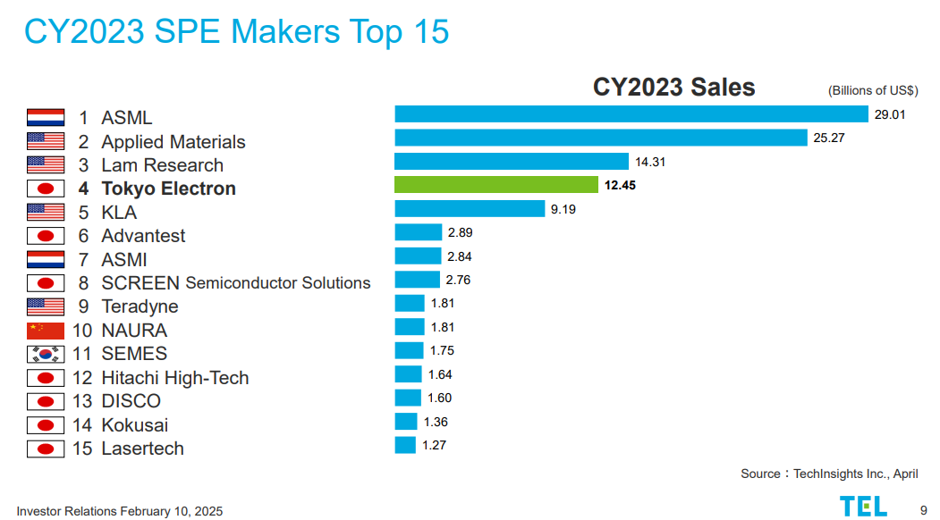
Tokyo Electron (TEL) is the 4th largest global supplier of semiconductor production equipment (SPE). It has a broad SPE portfolio similar to Applied Material, while peers like ASML, KLA and Lam Research are more specialized. The most dominant product in TEL’s portfolio is photoresist coater / developer system where they have a 90% market share. Throughout its history, TEL evolved through multiple phases – from importer to co-manufacturer, then to an independent equipment developer.
History
Tokyo Electron was founded in 1963 by Norio Kubo, a former Nissho Iwai trading company employee, with startup capital provided by Tokyo Broadcasting System (TBS). Initially, TEL operated as a distributor of imported electronic equipment – exporting car radios and importing semiconductor fabrication tools. Early on, TEL forged partnerships with U.S. manufacturers like Thermco (diffusion furnaces) and Fairchild Semiconductor, developing deep technical expertise in the operation of SPE.
In 1968, TEL transitioned into manufacturing SPE by forming a joint venture with Thermco to produce diffusion furnaces in Japan. TEL decided to withdraw from the export operation in 1974 due to strong yen post 1971 Nixon shock and 1973 oil shock. Subsequently, it formed joint venture with Lam Research to produce etching equipment and Varian Semiconductor (acquired by Applied Materials) to produce CVD and PVD equipment.
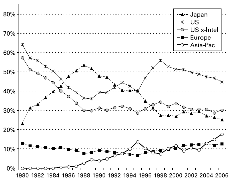
The next evolution came during the late 1980s semiconductor downcycle. As both Lam Research and Thermco were hit hard, they requested TEL to acquire their shares in TEL Lam and TEL-Thermco. TEL became a SPE company and was supported by customers such as Toshiba, NEC and Hitachi. This was at a time when Japanese manufacturers dominated the memory market with their higher yield rate and lower cost. From 1989 to 1991, TEL was the world’s biggest SPE producer. The Plaza Accord and the 1986 US-Japan Semiconductor Trade Agreement set the stage for the American semiconductor manufacturers to regain share in the 1990s (Intel also open a new market in microprocessor).
Source: Chips and Change
With the decline in the local semiconductor market, TEL started to develop a global footprint by cooperating with partners such as Varian in Europe, KLA in US and Hermes-Epitek in Taiwan. In 1994, the decision was made to switch to a direct sales model in its overseas market.
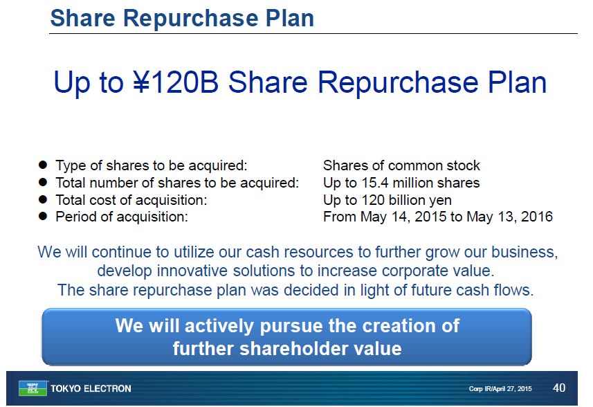
One final key development was the announced merger with Applied Materials in 2013. With the consolidation of memory and logic producers, Applied Materials wanted to consolidate to improve its bargaining power against the customers. While the merger was called off in 2015 due to anti-trust concerns, Tokyo Electron’s then CEO Tetsuro Higashi was inspired by Applied Materials focus on shareholder returns. A share repurchase plan of JPY 120 billion was announced in 2015 which reduced the total outstanding shares by 8% in year. 3 more share repurchase plans were announced in 2020, 2023 and 2024. Share repurchase is now an important source of shareholder returns for all major SPE companies today.
Source: Tokyo Electron
Revenue overview
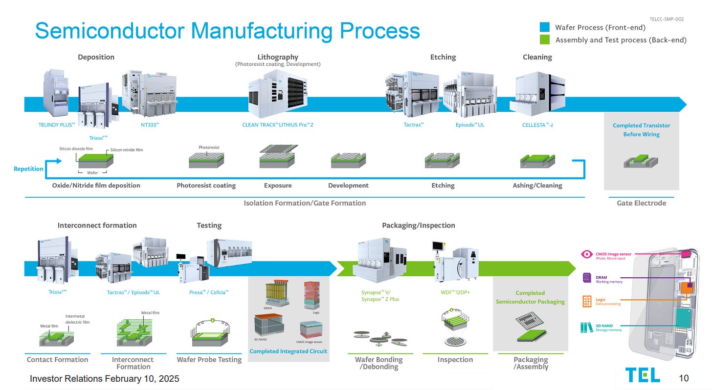
The company's product portfolio spans multiple key process steps in semiconductor production, including deposition (CVD, ALD, oxidation/diffusion furnaces), etching (dielectric and conductive plasma etch, including its latest cryogenic etch for 3D NAND), and cleaning (single-wafer and batch wet cleaning). TEL is also the undisputed leader in coater / developer systems, with a 90% global market share, making its track equipment integral to EUV and DUV lithography. It has also expanded into wafer bonding and debonding systems to address the growing demand for heterogeneous integration and advanced packaging.
Source: Tokyo Electron
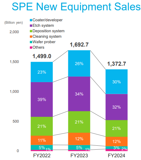
By revenue, the 4 key products (coater / developer, etch, deposition and cleaning) account for 95% of its product sales. Key clients such as TSMC, Intel and Samsung account for 50% of their sales.
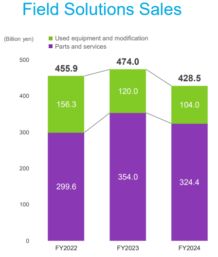
Field Solutions business, which contributes approximately 23% of total revenue, serves as a recurring revenue stream, providing a stabilizing counterbalance to the cyclical nature of new equipment sales. This segment encompasses servicing, spare parts, upgrades, and used equipment refurbishments, ensuring that TEL’s vast installed base of over 96,000 tools remains operational at peak efficiency throughout their lifecycle. Field Solutions sales have grown at a CAGR of 14% in the last 10 years.
Source: Tokyo Electron
Competitive Landscape
The SPE industry is dominated by a handful of large players, each with areas of specialization. Tokyo Electron is ranked #4 globally by revenue, alongside Applied Materials, ASML, and Lam Research. The SPE industry is highly consolidated with the top 5 companies accounting for 75% of the industry sales. ASML is the monopoly supplier of EUV lithography system and is a key partner of TEL. Lam Research is a dominant supplier of etching equipment and will be the most direct competitor to TEL over the next few years.
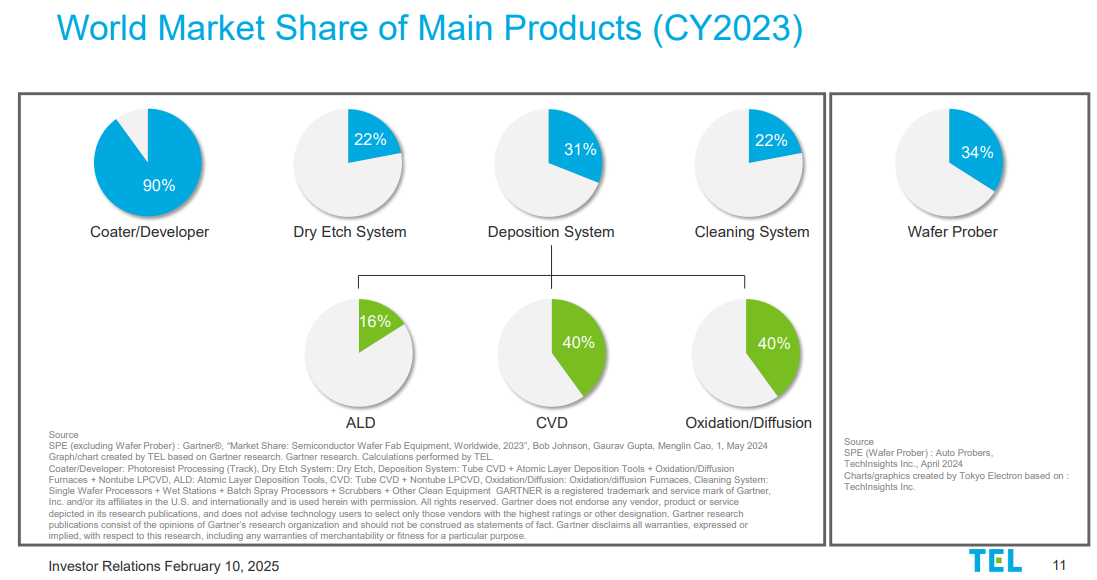
According to TEL’s estimates, it ranked No.1 worldwide in Coater/Developer tracks, Gas Chemical Etch systems, Diffusion furnaces, and Batch Deposition systems, and No.2 in Cleaning systems, Plasma Etch systems, Metal deposition, and Wafer Probers. This impressive breadth across critical process steps makes TEL a primary supplier to any leading-edge fab.
Source: Tokyo Electron
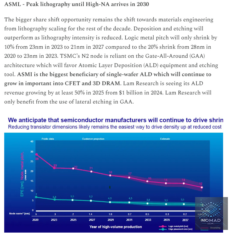
With peak lithography over the next 5 years, non-lithography SPE makers will benefit as deposition and etching gain share.
Now, we will examine their market share trajectory in the key products.
Coater / Developer - Tokyo Electron will defend its share against Lam Research’s Dry Resist
Coater / developer systems are used in the lithography process to coat wafers with photoresist before exposure and to develop the latent image after exposure. TEL is the undisputed world leader in this category with the CLEAN TRACK coater / developer systems (models like ACT, LITHIUS Pro).
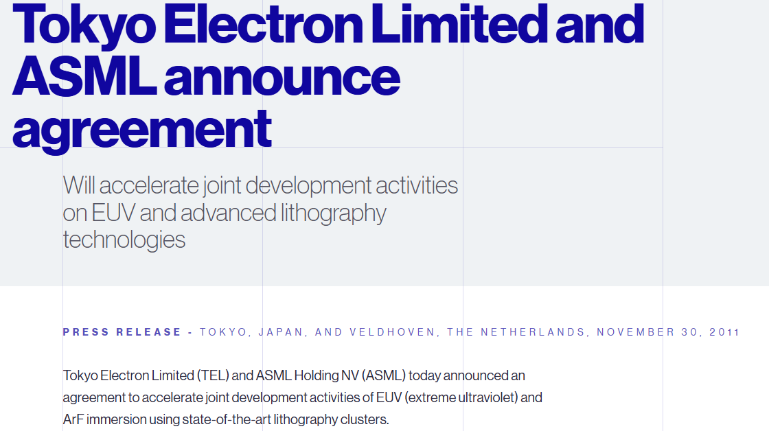
TEL holds 90% share of the coater / developer market and 100% share of the EUV lithography coater / developer market. TEL’s tools are tightly integrated with ASML scanners and their close partnership is a barrier of entry for new competitor. Key photoresist suppliers are also all Japanese firms (Shin-Etsu, JSR and TOK) which have close cooperation with Tokyo Electron.
This segment has been a steady cash cow for TEL, but it’s also at the forefront of a technical challenge due to emerging Dry Resist technology from Lam Research. CAR (Chemically Amplified Resist) is the conventional photoresist used in today’s lithography. It’s a liquid resist spun onto wafers by TEL’s coater. CAR has served well but is facing issues like stochastics and resolution limits as the industry migrates to 2nm and beyond.
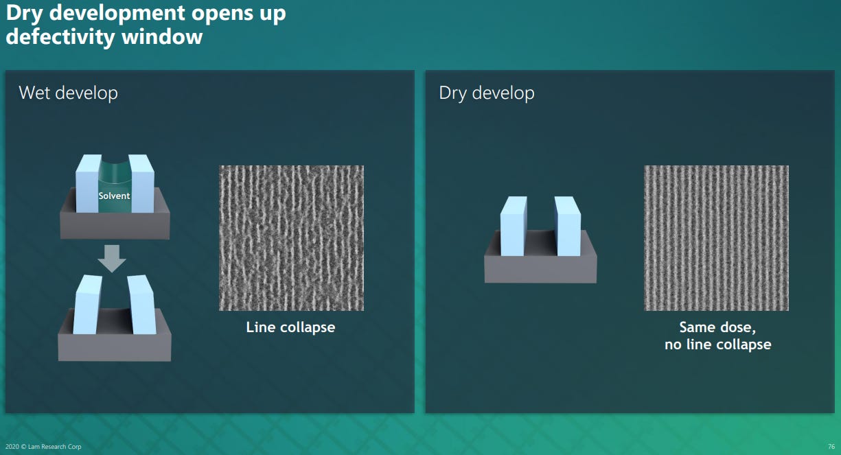
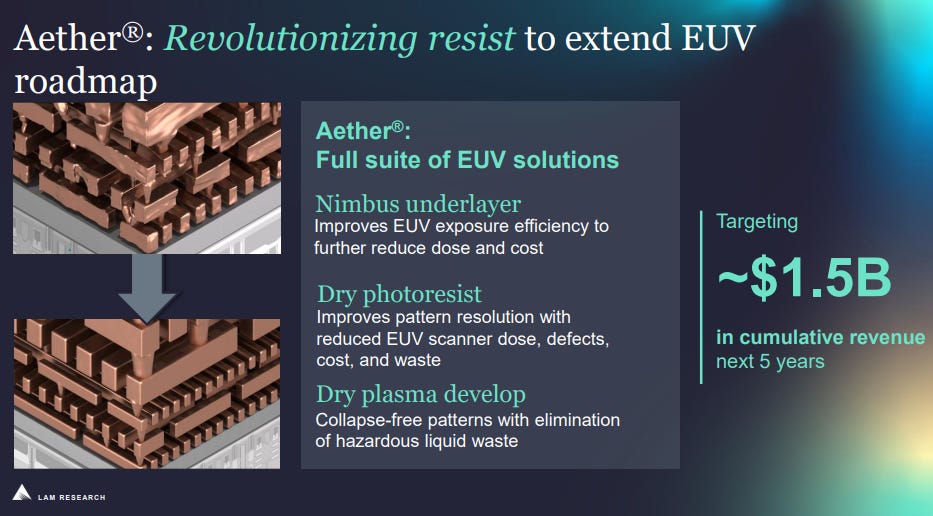
Lam Research unveiled a dry resist technology for EUV – essentially an ALD (atomic layer deposition)-based vapor-phase deposition process that deposits a resist film , rather than spin-coating. This dry resist can be extremely thin and achieve high resolution, potentially enabling 2nm patterning. Dry resist, being vapor-deposited, does not rely on liquid processing, thereby eliminating surface tension-driven pattern collapse. If dry resist were widely adopted, the lithography process flow might change – instead of a TEL coater applying resist, Lam’s tool would deposit it. That could disrupt TEL’s near monopoly in resist coating for the critical layers.
Source: Lam Research Investor Day 2020
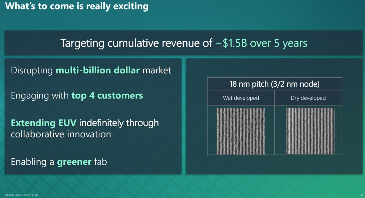
Despite the threat from Lam Research, they have yet to achieve the $1.5 billion revenue over 5 years target that they set in the 2020 Investor Day. In the 2025 Investor Day, Lam Research has the same target of $1.5 billion over the next 5 years. After 5 years, dry resist adoption is still slow as Lam Research has only announced 1 memory client. Dry resist requires new deposition and etching equipment which are much more expensive. The throughput is also lower as the cycle time may be longer compared to the high-throughput spin-coating process used for CAR.
Source: Lam Research Investor Day 2020
Source: Lam Research Investor Day 2025
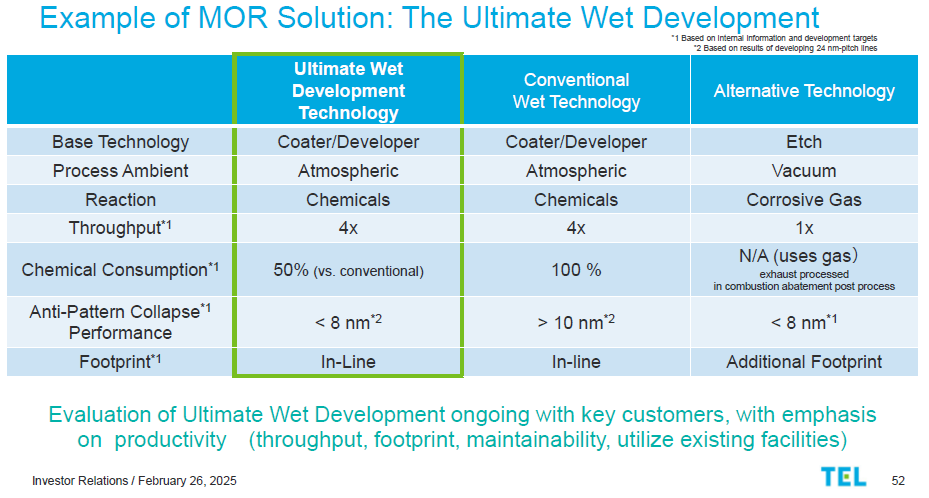
TEL is also not sitting still as they are developing the next generation wet resist process called MOR (Metal Oxide Resist). This is a newer inorganic resist pioneered by Inpria which had been acquired by JSR. MOR advantage is that it can achieve similar pattern integrity benefits while still being compatible with existing wet development processes, allowing fabs to avoid the extra cost of implementing plasma-based dry resist deposition tools. MOR process is able to prevent pattern collapse for resist pattern of 8nm which is similar to the dry resist process.
Source: Tokyo Electron Investor Day 2025
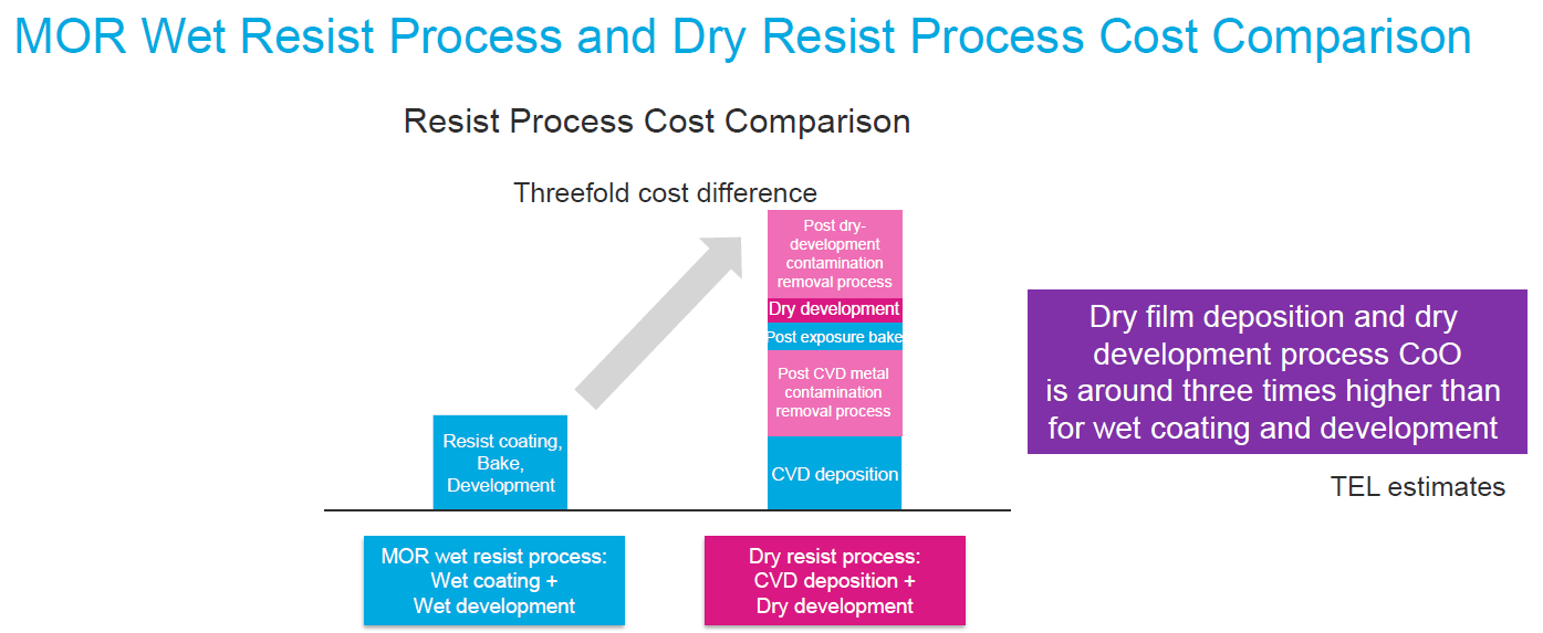
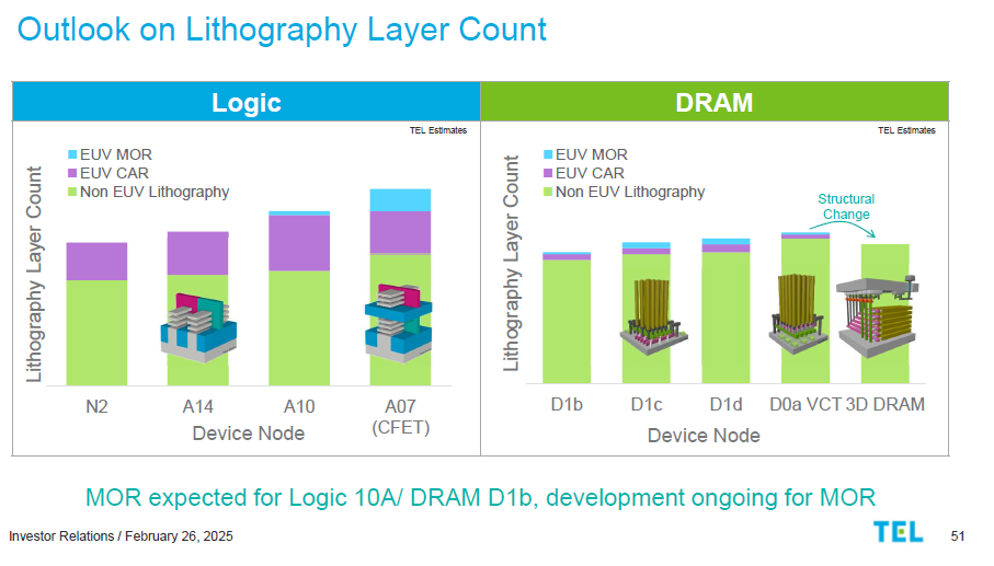
Given the 1/3 cost advantage over dry resist, MOR is expected to be introduced at 10A for logic and 1b nm for DRAM. This will effectively stop the share gain opportunity for Lam Research. SK Hynix is reported to have adopted MOR solution for 1c nm DRAM and Samsung is testing it too. TEL is also working with ASML on the coater / developer system for High-NA EUV at 10A.
Source: Tokyo Electron Investor Day 2025
Part 2 of the deep dive will look into deposition, cleaning, etching and bonder. It will explore some of the key growth opportunities for Tokyo Electron in etching and bonder.

